

Hardware & PCB Design
Schematics, PCB layout and enclosure design from our hardware lab in Chisinau, Moldova — engineered beside the firmware and software teams that will live with every routing decision. Boards from this bench run in shipped products, from workspace sensors to power-station electronics.
The free 30-minute session reviews your concept, sketch or existing board and gives an honest read on design effort, component risk and manufacturability. You keep the notes either way.
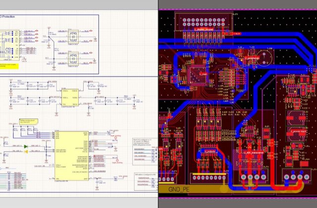
Where board projects go wrong
The prototype board cannot become the product board
The devkit-and-jumper-wires prototype proved the idea, and none of it survives contact with manufacturing: parts picked for availability that day, layout that ignores EMC, no test points. Productisation is a design discipline of its own — and the right moment for it is now, not after the crowdfunding video.
The chip on the schematic does not exist at volume
Component availability decides schedules now. We design with sourcing reality in view — second sources named, risky parts flagged, footprints chosen for alternatives — because a beautiful board you cannot populate is art, not engineering.
EMC failure discovered at the certification lab
A board that fails radiated-emissions testing after the enclosure is tooled is the expensive version of a lesson available cheaply earlier: EMC is a layout decision, made trace by trace, long before the test chamber.
Electronics and enclosure designed in different universes
The board is finished, then the case is designed, then the connectors do not reach and the thermals do not work. Board and enclosure are one design problem — we treat them as one deliverable.
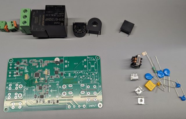
Every layout is graded twice: once by the EDA rules, once by the person assembling it downstairs. The second grade is stricter.
What the lab delivers
Schematics with reasoning
Circuit design documented with its trade-offs — power budgets, protection, sourcing risk — reviewed against the firmware it must serve.
You get: schematics your next engineer can read and question.
PCB layout for real conditions
Stack-up, routing, EMC discipline and thermal design for the environment the device actually meets — plus test points and programming access, because the board must be manufacturable and testable, not just correct.
You get: layout files ready for fabrication, with DFM checks done.
Enclosure and mechanical design
Cases designed with the board: connectors, thermals, assembly order, certification labels — prototyped in the lab before tooling money moves.
You get: an enclosure that fits the board, the hand and the production line.
Design for the whole lifecycle
BOM with second sources, assembly documentation, and the revision discipline that keeps hardware iterable.
You get: a design package a contract manufacturer can quote from directly.
How it works
Requirements and feasibility
Function, environment, certifications, cost targets — the constraints written down before the first symbol is placed.
Schematic and review
Circuit design reviewed jointly with firmware — pinouts, power, debug access — before layout begins.
Layout, prototype, test
Boards fabricated, assembled and exercised in our lab in Chisinau — bring-up, measurements, EMC pre-checks at the bench.
Revision to production
Findings folded into the production revision, with the design package handed over or carried into our assembly service.
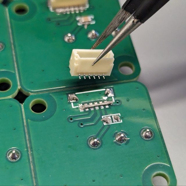
Board and firmware, one bench, one team.
Proof, not claims
The boards from this bench sit inside shipped products — and the lab does its own assembly, so designs answer to reality quickly.
Electronics for a power-station product line
Years of software and system work on a novel power station for PV systems — with the electronics discipline high-power products demand.
Design and assembly under one roof
Our hardware lab designs, prototypes, assembles and tests in one place — so layout decisions are graded by the same people who solder them.
A board designed next to its firmware team avoids the most expensive class of respin: the one caused by two vendors meeting at a connector.
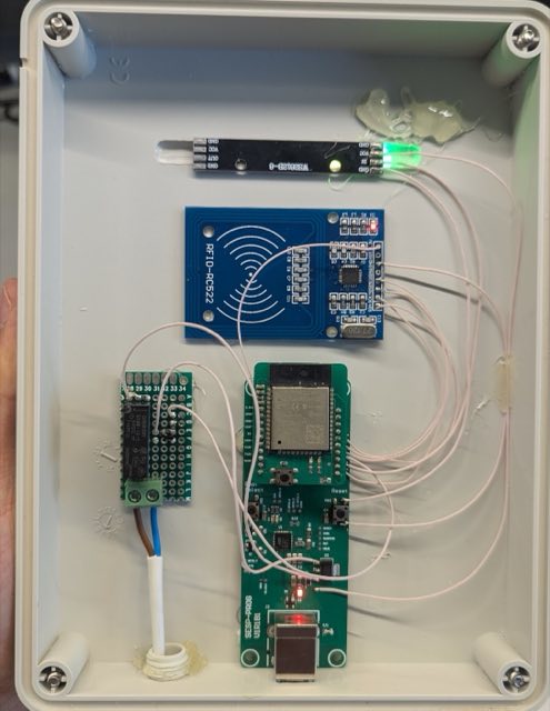
The case and the board are designed together — connectors that reach, heat that leaves, screws a production line will tolerate.
Put the concept on the bench
One 30-minute session with a hardware engineer: your concept, sketch or existing board, an honest effort-and-risk read, and the shape of a first design phase — priced in writing before anything starts.
Existing board with problems? The first phase is a design review with findings in writing — often the cheapest respin insurance available.
Clients also buy
Prototyping, Assembly & Testing
Prototype to small batch to FCC/CE/UL/RoHS testing — one lab, one accountable team.
Embedded Firmware
C++ firmware for machines that cannot fail — tunnel-boring machine control, solar power stations, industrial sensors.
IoT & Edge AI
Connected devices with on-device intelligence — from sensors to smart power stations, hardware and cloud in one team.
Good hardware looks inevitable in hindsight. Getting there is a hundred reviewed decisions per board — we write the reasons down.
The questions buyers actually ask
Where does the design work happen?
In our hardware lab in Chisinau, Moldova — schematics, layout, prototyping and assembly under one roof, working alongside our firmware and software teams. One accountable team from circuit to cloud is the point of the setup.
Can you take over a board someone else designed?
Yes — starting with a design review: schematics, layout, BOM risk and test coverage read by our engineers, findings in writing. Then a revision plan, prototyped and measured in the lab before production money moves.
How do you handle component shortages?
By designing for them: second sources named in the BOM, footprints chosen to accept alternatives, risky single-source parts flagged at schematic review. Sourcing reality is a design input, not a procurement surprise.
Do you design for certification from the start?
Yes — EMC discipline in the layout, creepage and clearance where voltage demands it, labelling and test access planned early. Certification testing itself runs through our Prototyping, Assembly & Testing service — FCC, CE, UL and RoHS paths included.
Can you do the enclosure too?
Yes — board and case are designed as one problem: connectors, thermals, assembly order and appearance, prototyped in the lab before tooling. A device is bought as an object, not a PCB.
What does a board design cost?
Scoped in writing after the free review — complexity, certifications and revision count drive the number. Fixed-price phases keep the spend approvable stage by stage.
From schematic to certified device — the one-page version
The Hardware & IoT Lab on one printable page: firmware, electronics, prototyping and certification testing, and how a device project moves through them. Built to be forwarded to whoever holds the budget.
From sketch to fabrication files
Book the free 30-minute review of your concept or board — or describe the device in two sentences and a hardware engineer replies in one business day.
- 30 minutes, an engineer on the call
- You keep the written notes either way
- Nobody follows up more than once